Release 0.1.0
sramforge
A memory compiler for a 7 nanometre process, built with open-source tools only.
Every chip needs memory, and memory is not written in a hardware description language like the rest of a design. It is drawn. A compiler takes the size you want and assembles the transistor-level artwork, because hand-drawing a few hundred thousand transistors is not an option. Those compilers are normally supplied by the foundry or bought, and they are closed.
This one is written in Python for ASAP7 (Arizona State Predictive Process Design Kit, 7 nanometre), an open kit for a 7 nanometre process. Like a foundry's compiler, it starts from cells it did not draw: the memory cell, the sense amplifier, the write driver and the other leaf cells come from the kit's own SRAM (Static Random-Access Memory) release, published under a BSD (Berkeley Software Distribution) licence. The compiler builds everything around them, and then checks the result, from whether every shape is in place to whether the block stores data in time.
Configuration space
A compiler builds a memory block to a requested size rather than supplying one fixed block. Three parameters set the size: the number of bits, the number of strips and the number of rows. Every combination the controls below allow can be generated. The reference size has passed every check, and Verification states which checks were run on the other sizes.
Where one word lives
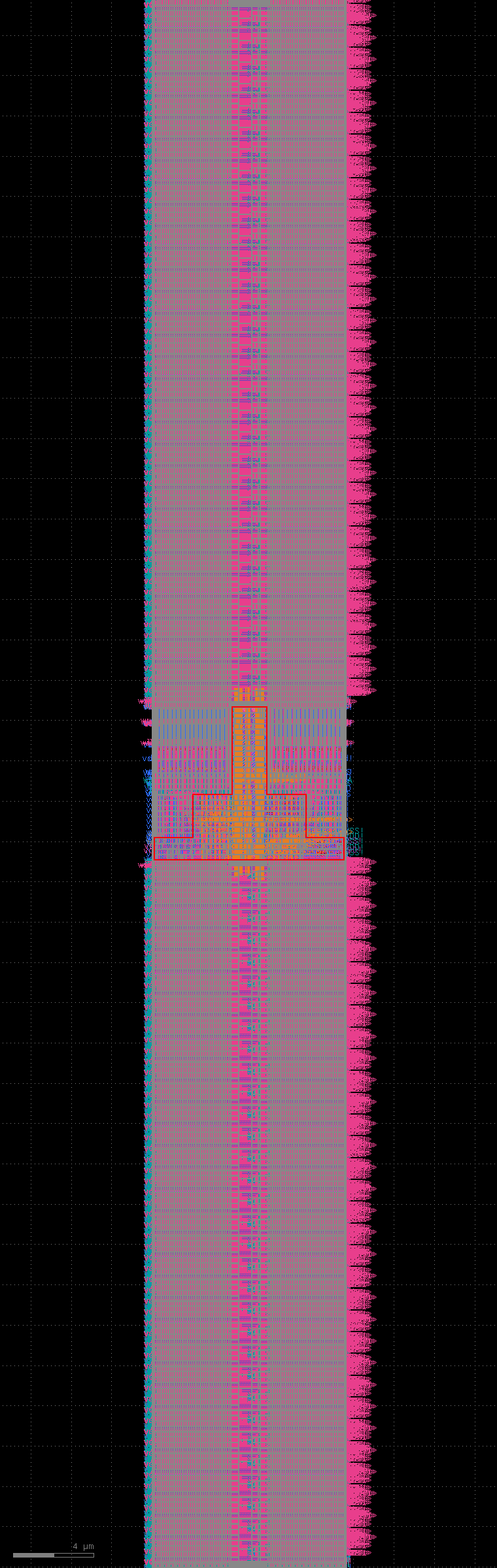
A word is not a run of neighbouring cells. Every column group holds one bit of it, always in the same place, so a word is a single vertical thread through the whole block. Here it is in the artwork, at three magnifications of one generated 2 kilobyte block.
The whole block

9.61 by 77.80 micrometres. The amber line is the word's column of cells: full height, both halves, stopping at the band. Pale blue is memory cells, green the shared read and write column, slate the decoder and control. The marker is twice the column's true width, to be visible.
One column group

Both sides of it: two arrays of 32 cells, four tall, sharing one read and write column. That sharing is what makes them one group, giving one bit.
One cell
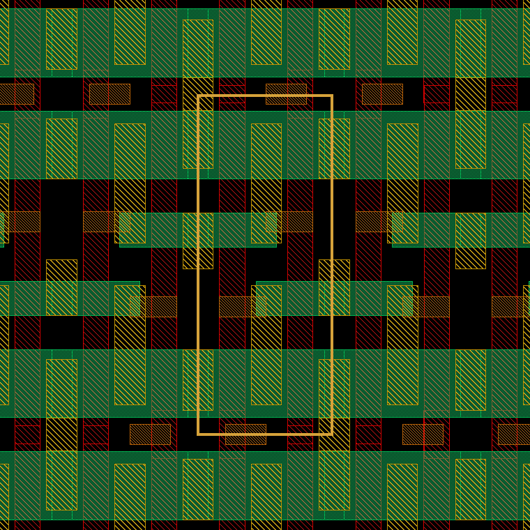
Six transistors in 0.108 by 0.27 micrometres. Two cross-coupled inverters hold the bit for as long as the supply is on, and the two access transistors join it to the bit lines when the word line rises.
Any size, drawn
The same two drawings for any size the compiler will build: the block with the word's column marked, and one of its groups.
What an address means
What each part of it selects, from the block down to one cell in every group.
One read
From the signals at the edge of the bank to data on the pins. Step through it with the arrows, which stay in view as you scroll the drawing.
One write
The same bank, storing a bit instead of reading one: the write driver takes the place of the sense amplifier.
At the cell: a read and a write
Inside one cell: six transistors, two bit lines and a word line. Pick read or write and step through what each part does. The gauge beside each bit line shows its voltage, from 0 to 0.7 volts.
Generation
The compiler draws no transistors of its own. It works from four items the kit publishes:
Generation proceeds in four steps.
1. Measure the rules
The kit publishes the finished reference block, but not the placement rules that produced it. The rules were therefore recovered from the block itself: its cell hierarchy was traversed level by level, and the position and orientation of every placed instance were recorded. The four drawings show the result, from the smallest level upward. The amber numbers are measured offsets and pitches in micrometres, and every drawing is to scale.
Replayed at the reference size, these rules reproduce the block shape for shape on all 31 mask layers; that identity is the first verification question. Every other size is generated by replaying the same rules with different counts.
2. Tile to the requested size
The generator applies the measured rules level by level, from a single cell to the complete block, and the three parameters change the counts it applies them with. The animation below shows the process to scale. Its geometry is computed from the generator's own placement code, measured values appear in amber, and it can be played or stepped through.
Each level also contains shapes that the kit drew outside any cell: supply straps, seam connectors, pin labels and rule markers, about 50 shapes and 370 labels in total. Without them the identity check fails on 13 layers and every bit line is open. They are stored as a table that can be reviewed, and each parameter has a rule for how they change:
| Parameter | Effect on the loose shapes |
|---|---|
| Bits above 32 | Shapes beside the array move outward, and the metal of one column pair is copied for each additional pair |
| Bits below 32 | The word line labels of the empty columns are removed |
| Eight strips | Shapes that span a group's height stretch with it, and the bit line labels are copied for the new strips |
| Rows | Shapes at a stack's outer edge move with it, and the data pin labels are regenerated for every row |
3. Rebuild the control
The control logic in the central band latches the address, enables the decoders, selects the column and times the sense amplifier. The kit provides it as a single hand-packed block drawn for the reference size. That block has no spare address input, and its delay line reaches only 277 picoseconds, so it supports only sizes close to the reference: 32 bits, four strips and up to 48 rows. For all other sizes the compiler rebuilds the control in five stages:
- Recover197 gates, 147 nets The kit provides the control only as drawn shapes. Its netlist is recovered from them with the connectivity extractor that the checks use, by probing each gate's pins for the wire beneath them. Every pin resolves to a net, and the block's 37 ports are taken from its own pin labels.
- Edit348 gates New logic is added: a delay line of up to 62 buffer pairs, a ninth address bit, the enables for a second decoder bank at 64 bits, and the select drivers for the right array. The eight-strip variant adds a 3-to-8 column decoder, for 412 gates.
- Floorplan9.4 by 9.0 micrometres The rebuilt control occupies a full-width region beneath the decoders, which makes the band 7.6 micrometres taller. Each original pin is placed exactly on its former pad, and 1,979 shapes of the band's overhead wiring become obstructions for the router.
- Place and routeby OpenROAD Power rails run along every row, cells are placed at 45 per cent density, and global and detailed routing use metal layers 2 to 4. Band wires that must cross the region are routed through it as additional two-point nets. Any route that contains a short is rejected.
- Merge and checkone wire per word line The routed region is inserted back into the band with generated wiring around it: supply straps, via stacks down to the original pads, and short stubs that join crossing wires to their routes through the region. Connectivity, decoding and simulated reads and writes are then checked again.
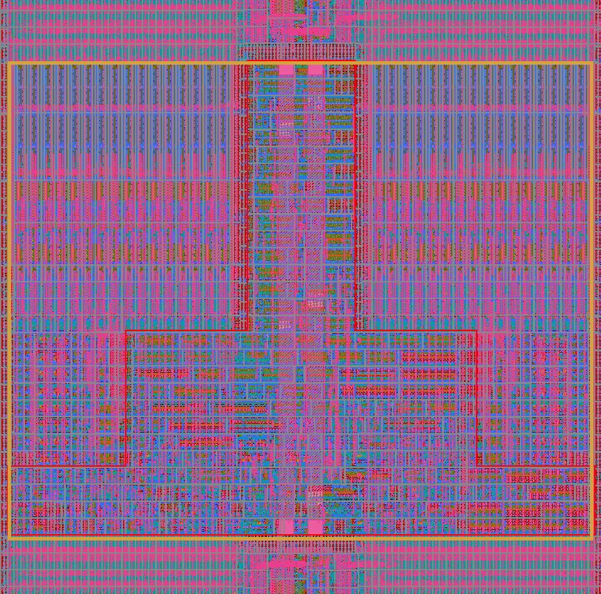
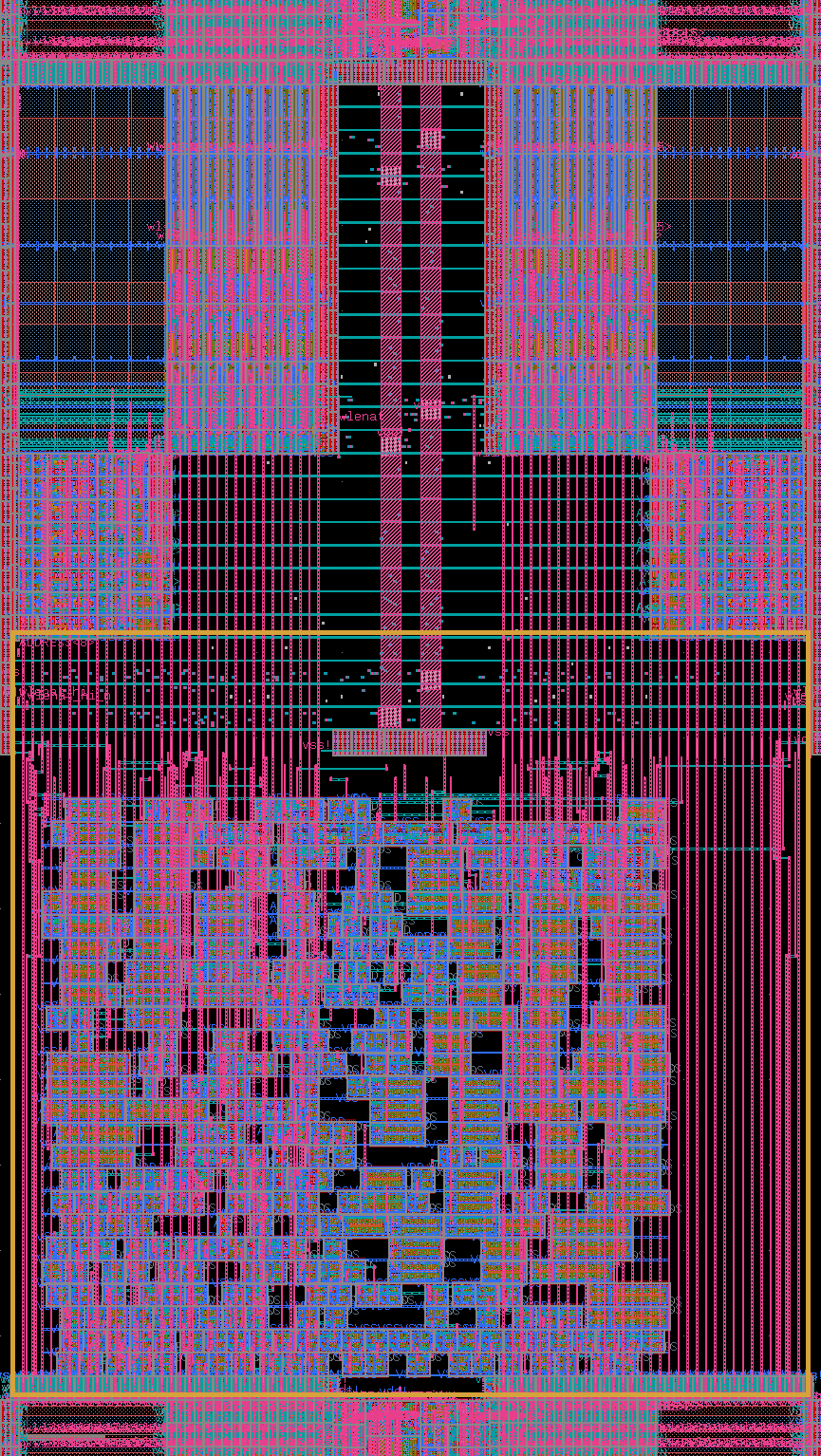
The rebuild was also the source of the project's most serious defect. The first extraction omitted the right array's select drivers, which left half the words of every rebuilt block unreachable until a more detailed check detected it.
4. Time the sense amplifier
The sense amplifier must not fire until the selected cell has pulled its bit lines far enough apart to be read, and that time depends on the block's size. The generator computes it as the sum of four parts, each measured in simulation:
- Clock to word line. The control raises the word line 83 to 92 picoseconds after the clock edge, depending on which control the block uses.
- Word-line flight. The word line is a long wire, and its far end rises last. This delay grows with the square of the wire's length, so it is the part that varies most with size.
- Bit-line split. The cell then pulls its bit lines 100 millivolts apart, in 18 to 30 picoseconds depending on the width.
- Margin. A fixed 20 picoseconds.
The wait itself is produced by a delay line in the control. The line
is a chain of ordinary logic gates, not an analog circuit: its delay is
the time a signal takes to pass through the gates. It is selected by the
block's five sdel pins and measured by transistor-level
simulation of the block's own extracted layout. The line as the kit
draws it, and as the rebuild makes it:
sdel pin. A gate whose bit is 1 passes the start signal straight on; a gate whose bit is 0 passes the slower path from the gate before it, through a buffer. The first 1, counting from sdel<0>, therefore sets how many gates the signal passes through, and sdel<4> has no effect: 6 settings, 204 to 277 picoseconds, each additional gate adding the amber amount.The generator selects the shortest setting whose delay covers the total. Hovering over a row, or moving to it with the Tab key, shows its parts.
The numbers, in picoseconds
| Block | Control | Clock to word line | Far end of the word line rises | Bit lines split by 100 millivolts | Margin | Needs | Setting | Waits |
|---|---|---|---|---|---|---|---|---|
| 8 rows | kit's control | 88 | 20 | 22 | 20 | 149 | 11111 | 204 |
| 16 rows | kit's control | 88 | 30 | 22 | 20 | 160 | 11111 | 204 |
| 16 bits, 32 rows | rebuilt control | 83 | 73 | 18 | 20 | 194 | 11111 | 242 |
| 32 rows | kit's control | 88 | 73 | 22 | 20 | 202 | 11111 | 204 |
| 48 rows | kit's control | 88 | 142 | 22 | 20 | 272 | 00000 | 274 |
| 64 rows | rebuilt control | 83 | 239 | 22 | 20 | 364 | 11011 | 411 |
| 64 bits, 64 rows | rebuilt control | 83 | 239 | 30 | 20 | 372 | 11011 | 411 |
| 8 strips, 32 rows | rebuilt, eight strips | 92 | 239 | 22 | 20 | 373 | 11011 | 410 |
| 96 rows | rebuilt control | 83 | 514 | 22 | 20 | 640 | 10101 | 668 |
| 8 strips, 64 rows | rebuilt, eight strips | 92 | 899 | 22 | 20 | 1033 | 00110 | 1049 |
Two results follow from the chart. Beyond 48 rows no setting of the kit's line waits long enough, which is why deeper blocks receive the rebuilt control. The rebuilt line's shortest delay is 242 picoseconds, so a small block that uses it, such as the 16-bit one, waits longer than necessary. Each build records the setting for both the typical and the slow corner, and a check under Verification confirms that every size it covers has one.
Outputs
Each build writes the files needed to place, time and simulate the block within a chip design. All of them are derived from the same layout and from one shared list of its pins, so they agree on the block's interface by construction; a check also confirms that the pin names match across them.
Pin names, directions and layers come from the contract. Shapes come from the layout, and numbers from simulating it.
The pin contract
The ten pin families of the 2 kilobyte block:
ADDRESS[7:0], input, metal 5: which word: the bits split into column, word line and half. Eight bits here, nine on every other size.clk, input, metal 5: the clock: an access starts on its rising edge.banksel, input, metal 5: enables the block; while it is low nothing happens.read, input, metal 5: read enable.byte_wrenab, input, metal 5: write enable.sdel[4:0], input, metal 5: the sense amplifier's delay setting, tied to the value the manifest names (step 4 of Generation).wd[63:0], input, metal 3: write data, one pin per column group.dataout[63:0], output, metal 3: read data, latched and held between reads, one pin per column group.VDD, power, metal 3: the supply: one pin made of two pieces of metal.VSS, ground, metal 3: ground.
In total the block has 147 pins: 8 + 1 + 1 + 1 + 1 + 5 + 64 + 64 + 1 + 1.
The abstract
A place-and-route tool does not need the block's transistors. It needs the block's outline, the position and metal layer of each of its 147 pins, and the areas in which it must not route. The abstract provides exactly that. It is derived from the layout: each pin is the metal beneath one of the layout's pin labels, and the blockages are the layout's own metal, merged. A check confirms that the pins and blockages together cover the drawn metal exactly, and rejects damaged abstracts.
Drawn from the abstract file itself. Metals 1 and 2 are blocked over almost the entire block (47,095 and 26,025 merged islands), so only the upper metals are shown. The control and address pins are stripes on metal 5 above the central band, and each column group brings out its write-data and read-data pins on metal 3.
The timing library
A timing tool must know when the block's inputs have to arrive and when its outputs change, without simulating the block. The timing library, in the Liberty format, records both, and every value in it was measured by simulating the block's extracted layout. One read as the library describes it, at the typical corner, in picoseconds:
The address must be stable 45 before the
clock edge and 30 after it. Inside the block, the word line
rises at 87 and the sense amplifier fires at
205; neither appears in the library, which describes only
the pins. The word appears on dataout 243 after
the clock, and the next read can begin 516 after this
one, which corresponds to 1.94 gigahertz. Write data is the
exception: it may arrive up to 18 after the clock edge,
but must then remain stable for 40.
Delays are stored as tables. A timing tool looks up the slew of the
clock it sees and the load on the pin, and interpolates between the
entries. Clock to dataout, rising, in picoseconds:
| clock slew | 5 fF | 20 fF | 50 fF |
|---|---|---|---|
| 20 ps | 243.3 | 254.5 | 275.4 |
| 60 ps | 250.6 | 261.8 | 282.6 |
A timing tool has read this library together with the abstract and met timing at the 516 picosecond period; question 7 of Verification describes the run. A few values are estimates rather than simulation results, chiefly the wire component of each input pin's capacitance, and the characterization record marks each of them. The resistance and capacitance of the block's internal wiring are not included in the simulations.
The behavioural model
Simulating a chip that contains the block requires only a fast model of its behaviour. The Verilog model is generated from the same pin list, with the address map measured from the layout: which address bits select the column, the word line and the half.
// Behavioral model generated by sramforge.
// Single-port (one read/write port) SRAM (Static Random-Access Memory):
// 256 words x 64 bits, 8 address bits.
// Port names and widths follow docs/pin_interface.md, the same contract
// the LEF (Library Exchange Format) abstract of this bank is written from.
// Measured address map: ADDRESS[1:0] = column-mux select,
// ADDRESS[6:2] = wordline column, ADDRESS[7] = half select.
// Column codes >= 32 have no cells in the layout (sparse-bits scheme):
// a write there is dropped and a read returns x.
module sramforge_32bx4x64 (
      input                  clk
    , input      [7:0]     ADDRESS
    , input      [63:0]    wd            // write data
    , input                  banksel       // access enable (active high); nothing happens when low
    , input                  read          // read enable
    , input                  byte_wrenab   // write enable
    , input      [4:0]       sdel          // sense-timing delay-line code: accepted, functionally ignored (tie to 5'b11111)
    , output reg [63:0]    dataout       // read data, latched; holds between reads
);

  reg [63:0] mem [0:255];   // 256 address codes, 256 implemented

  wire [4:0] column = ADDRESS[6:2];
  wire live = (column < 32);         // the column exists in the layout

  always @(posedge clk) begin
    if (banksel & byte_wrenab & live)
      mem[ADDRESS] <= wd;
    if (banksel & read)
      dataout <= live ? mem[ADDRESS] : {64{1'bx}};   // held until the next read
  end

endmodule // sramforge_32bx4x64
The manifest
Finally, a short record of what was built: its size and organization,
and the delay-line setting to which the sdel pins should be
tied at each corner.
{
  "top_cell": "sramforge_32bx4x64",
  "bits_per_group": 32,
  "strips_per_group": 4,
  "depth_groups": 32,
  "bitcells": 16384,
  "width_um": 9.612,
  "height_um": 77.804,
  "reference_exact": true,
  "data_bits": 64,
  "num_words": 256,
  "address_bits": 8,
  "sense_timing": {
    "TT": {
      "code": "11111",
      "need_ps": 202.3,
      "sae_ps": 203.6,
      "slack_ps": 1.3
    },
    "SS": {
      "code": "11111",
      "need_ps": 217.1,
      "sae_ps": 237.8,
      "slack_ps": 20.7
    }
  }
}
Measured results
Every number below is measured on the generated layout: the area from its outline, and the rest by simulating the transistors extracted from it at the typical corner. Each is reproducible from the repository. The simulations leave out the resistance and capacitance of the wiring, and the idle power is scaled up from measured slices of the block. The values are for the 2 kilobyte block shown above.
| Property | Value | Meaning |
|---|---|---|
| Size | 747.9 square micrometres | 63.9 per cent of it is memory cells; the rest is the surrounding circuitry |
| Speed | 1.94 gigahertz | A 516 picosecond period: the 430 confirmed in simulation, plus a fifth as margin |
| Read latency | 243 picoseconds | From the clock edge to data on the output pins |
| Read energy | 0.615 picojoules | Charge drawn from the supply for one access |
| Idle power | 773 nanowatts | Leakage while the block is idle |
| Cell stability | 154 millivolts | The noise a stored bit tolerates while being read, out of a 700 millivolt supply |
The largest block taken through the same measurements holds 65,536 bits.
Verification
The block has never been made in silicon, so every answer below comes from the generated layout itself: the shapes it is made of, the wiring and transistors read back out of them, and simulations of those transistors. Seven questions, each relying on the ones before it:
- Is every shape where it should be?At the reference size the layout is identical to the kit's own block on all 31 layers. At every size, an independent program confirms the position and mirror of every cell.Proven on identical to the kit: the reference. Cells in place: 14 sizes
- Is it wired the way it should be?Rebuilding the wiring from the raw shapes finds every bit line, word line and supply as one unbroken wire, and no two wires touching.Proven on the reference and eight strips; 16 and 64 bits checked once
- Can it be manufactured?97 rules from the kit's rule manual, the checks a foundry would run before making it.Proven on the reference passes every rule. The other sizes still break some in known places, recorded so that no new one can appear
- Are the transistors the ones we meant?Every transistor is pulled back out of the shapes: each cell matches the six-transistor schematic, and all 114,454 in the block are accounted for.Proven on the reference; transistor counts cross-checked for 16 and 64 bits
- Does it store and return data?A simulation of the extracted transistors shows every address opening exactly the right cells and column, and a transistor-level simulation writes bits into cells and reads them back on the data pins.Proven on selection: the reference, with 16 bits, 64 bits and eight strips checked once. Write and read back: the reference, and every width from 4 to 32 bits checked once
- Does it work in time?The read is simulated at transistor level on the extracted layout and confirmed by simulating reads back to back; every size's sense amplifier waits for its farthest cell.Proven on read timing: the reference. Sense timing: 13 sizes
- Do the files a chip designer uses tell the truth?The abstract matches the layout exactly, every value in the timing library traces to a measurement, and a timing tool accepts both.Proven on abstract: the reference, 16 and 64 bits. Timing library: the reference
1. Is every shape where it should be?
Same as the kit's block. At the reference size the generator must reproduce the kit's published 2 kilobyte block exactly. Both layouts are flattened and, on each of the 31 mask layers, compared with an exclusive or (XOR): whatever is in one layout but not the other is left over. The check passes only if nothing is left on any layer, which shows that the measured rules of "Generation" are exact at that size.
What is left over is the area that one layout covers and the other does not. In the first row the two are identical and nothing is left: the pass. The second row shows what the check is for. It gets one constant of the strip recipe wrong by 18 nanometres, the offset of the first upright cell, so every upright cell in every strip sits 18 nanometres to the right of where the kit has it, and the check fails.
The drawing is computed from the two real layouts, the active and gate layers of a few cells in the first strips. The real check does the same on all 31 layers of the whole block.
Every cell in place. The identity check only works at the reference size. At every size, a second program, written apart from the generator and using none of its code, works out from the measured constants where every memory cell should sit and which way it should face. The cells found in the generated layout must match that list exactly: none missing, none extra, none out of place or mirrored the wrong way. It runs on 14 sizes: every width from 4 to 32 bits, depths from 4 to 64 rows, and eight strips.
When this check was written, a shifted strip, deleted tap cells and a flipped mirror were each tried once by hand and caught. Those trials were not kept as a repeatable test.
2. Is it wired the way it should be?
Shapes are not wires yet. A bit line is many separate shapes on different layers, joined where they overlap or where a via drops from one layer to the next. The check rebuilds the wiring from the raw shapes, the way the chip would conduct: it merges the touching shapes on each layer, splits a transistor's active area where its gate crosses it, joins the layers through every via and overlap, and then reads off which wire each of the layout's labels sits on.
Two things must then hold. Every wire must be whole: all the cells along a strip on one bit line, each word line one wire from end to end. And no two wires may touch: bit lines, their pairs, word lines, supply and ground all separate. On the reference block that is 512 bit lines and 512 pairs, 64 word lines, one supply and one ground, and the 16 column-select lines each on its own wire.
Drawn from the real extraction of one column group, metals 1 to 3. The damaged copies are made for this drawing, and the extraction is run again on each: the open and the short are what it reports. A gap and a bridge were also tried on the whole block when the check was written, and both were caught.
3. Can it be manufactured?
A foundry only makes a design that obeys its rule manual: how narrow a wire may be, how close two wires may sit, how far a via must land inside the metal it joins, and much more. The check transcribes 97 of the kit's rules, across 19 layers and layer pairs, and measures every shape of the block against them.
The figure shows one of them. In the memory array each bit line is a metal-2 wire 18 nanometres wide, the narrowest the manual allows, with 29.5 nanometres to the wire beside it, where the manual asks for at least 18. Widen it along a short stretch until the gap is under the minimum, and the check reports exactly there.
Memory is packed tighter than ordinary logic, and in places the kit's own block goes below the printed value of 31 rules. For those, the check uses the kit's tightest value instead: no block may be packed tighter than the kit's own. Where that leaves each size:
Ready to manufacture: the 2 kilobyte block. It passes every rule.
Not yet: the 1, 4 and 8 kilobyte blocks. They break a rule in 109, 110 and 678 places, almost all where new wiring had to be added. Every place is recorded and the check fails if a new one appears, but they are not fixed, and most are not yet individually explained. Most of the 8 kilobyte block's are one problem repeated, a via not sitting fully on its metal, which an outside checker confirms is real.
The figure is computed: the real rule check is run on one column group, as built and with the wider bit line. Not checked at all: a few rules that need more than the shapes, such as spacings that depend on which wire a shape belongs to, and the distance from a transistor to its nearest well tap.
4. Are the transistors the ones we meant?
A layout does not list its transistors: they exist only where shapes overlap. The check finds them the way the physics does. A transistor is wherever a gate crosses an active region, except where a gate cut severs the gate. The implant over it says whether it is n-type or p-type, and its strength is its fin count, the number of fins it crosses. Its connections come from the wiring rebuilt in question 2.
The memory cell must then match its schematic exactly: two inverters feeding each other, whose outputs Q and QB are the cell's two sides, and two access transistors joining those sides to the bit lines, all with the right types, fin counts and connections. After that the whole block is counted. The reference block holds 114,454 transistors. Its 16,384 cells account for 98,304 of them, six each: 65,536 n-type with 2 fins and 32,768 p-type with 1, exactly as six per cell requires. The other 16,150 are in the dummy cells, the read and write columns and the control. Every word line drives exactly 512 access transistors, and every bit line touches exactly 32.
Drawn from the real extraction of the kit's memory cell. The check also breaks the cell on purpose, swapping the n and p implants, deleting a gate cut and deleting a contact, and each must break the match.
5. Does it store and return data?
Two things have to work for a memory to hold data: each address has to reach exactly its own cells, and those cells have to take a bit and give it back. The first is checked by simulating the extracted transistors as switches. Every address is presented in turn, with a clock edge, and the decoder's outputs are read: exactly one word line may come on, and it must be the one the address map names.
The block has 256 addresses but only 64 word lines. The two least significant address bits select one of the four strips that share a word line; they do not change which word line is driven. Each row of the grid therefore represents four addresses. The same switch-level simulation also verifies the strip selection, that a write activates the write driver rather than the sense amplifier, and that the block stays inactive when it is not selected.
A switch-level model cannot represent the charge stored in a cell, so the second check is a transistor-level simulation. One column is taken from the extracted layout, comprising the cells, the write driver, the sense amplifier and the output latch, and simulated with the kit's transistor models. A 0 is written into a cell that holds a 1, and the cell is then read.
The recorded run of the 1 kilobyte (16-bit) block, from 20 July 2026. The cell's two sides cross over during the write, and on the read the data pin falls to the bit that was written. Both directions passed at every width from 4 to 32 bits that day; the control has been rebuilt since, and the runs have not been repeated.
How the simulations are run
Both checks simulate the layout itself rather than a schematic drawn by hand. The layout is first converted into a list of transistors and the nets that connect them, and the simulators run on that list.
- Extraction. A transistor exists wherever a gate crosses active area. Its type is read from the implant layer over it, its threshold flavour from the threshold-voltage marker, and its width from the number of fins it crosses; the active area on either side forms its source and drain. Each conducting layer, from the diffusion contacts up to metal 5, is merged and joined to the next through its vias, which assigns every transistor terminal to a net. The pin labels in the layout name the nets. This is the same extraction that question 4 compares against the intended transistors.
- Switch-level simulation. For the address check, each transistor is treated as a switch: an n-type device conducts when its gate is 1, a p-type device when its gate is 0. At every step, nets joined through conducting switches take the value of the supply or input they reach, and a net that reaches none keeps its previous value, as a charged node does. This shows which word line each address drives, but it carries no voltages and no times.
- Slicing. The full block, 114,454 transistors, is too large for an analog simulator, so only the circuit that can affect one data output is kept. Starting from the output pin, the slice grows backwards: a transistor joins if its source or drain touches a net already in the slice, and its gate net then joins as well. For the 16-bit block this gives 878 transistors: the bit lines with their cells, the column multiplexer, the write driver, the sense amplifier and the output latch.
- The circuit file. Each transistor in the slice becomes one line of a SPICE (Simulation Program with Integrated Circuit Emphasis) netlist, written directly from the extraction. The control signals at the edge of the slice (word line, write enable, bit-line precharge, sense enable) are driven by piecewise-linear voltage sources, with edge times measured in a separate simulation of the extracted control circuit. Every cell starts with a stored value, and the addressed cell starts with the opposite of the bit to be written.
- Simulation. ngspice solves the circuit over 6 nanoseconds with the kit's BSIM-CMG (Berkeley Short-channel Insulated-Gate Field-Effect Transistor Model, Common Multi-Gate) transistor models, at the typical corner and 0.7 volts. The figure above plots the voltages it recorded on the word line, write enable, sense enable, the addressed cell's two storage nodes and the data output.
N0 nm2_8597 nm3_51 nlig_14524 0 nmos_sram nfin=2
One line of the recorded circuit file: an access transistor of a cell in the top half. Its drain is on the complement bit line, its gate on word line 0 of the top half, its source on the cell's storage node and its body at ground, and it has two fins. The net names come from the extraction: nm2_8597 is net 8597, first found on metal 2.
The extraction yields transistors and their connections, not the resistance and capacitance of the wires. The bit lines are therefore loaded by the transistors on them but not by their metal, and the timing shown here is likely somewhat faster than the real circuit would be.
6. Does it work in time?
A read has two halves. While the clock is high, the word line opens the cells, the bit lines split and the sense amplifier decides, until the word is valid on the data pins. While it is low, the bit lines are pulled back up, ready for the next read. Both were measured at transistor level on the extracted layout, and their sum was then confirmed by simulating two reads back to back. A fifth is added on top as margin.
That gives 1.94 gigahertz at the typical corner and 1.67 at the slow one. The fast corner's simulations did not converge, so it has no number. As in question 5, the wiring's resistance and capacitance are not simulated, so both periods are likely somewhat optimistic. Every size also has to time its sense amplifier for its own farthest cell: step 4 of Generation shows how, and that check runs on 13 sizes. The read timing above was measured on the reference block only.
7. Do the files a chip designer uses tell the truth?
A designer never sees the layout itself, only the abstract and the timing library. So the abstract is checked against the layout: its pins and blockages, merged, must cover exactly the metal the layout draws, on every metal layer. Exported again here and compared on the central band:
The check also refuses an abstract whose layout has a pin label deleted, moved off its metal, or used twice. The timing library is checked differently: every value in it must trace back to a field of the measurement record, and the library says which. Its delay table, beside the record it was written from:
/* clk -> dataout: measured on dataout[0] (the
   characterized column), the cycle-2 edge of a two-
   read simulation; rows = clk input slew, columns =
   dataout load (read_access.cell_*_ps and
   *_transition_ps) */
timing() {
  related_pin : "clk";
  timing_type : rising_edge;
  timing_sense : non_unate;
  cell_rise(delay_2x3) {
    index_1("0.0200, 0.0600");
    index_2("0.005000, 0.020000, 0.050000");
    values("0.2433, 0.2545, 0.2754", "0.2506, 0.2618, 0.2826");
}{
"read_access": {
"input_slew_ps": [20, 60],
"load_ff": [5, 20, 50],
"cell_rise_ps": [
[243.3, 254.5, 275.4],
[250.6, 261.8, 282.6]
]
}
}The library stores nanoseconds and picofarads, the record picoseconds and femtofarads: 0.0200 is 20, 0.005000 is 5 and 0.2433 is 243.3. The abstract was checked on the reference, 16-bit and 64-bit blocks; the library on the reference.
Finally, both files were given to the tools a designer would use. OpenROAD loads the abstracts of the 16, 32 and 64-bit blocks as placeable blocks of the expected size and pin count; the 2 kilobyte block is 9.612 by 77.804 micrometres with 147 pins. OpenROAD refuses the exact abstract, drawn on a quarter-nanometre grid, alongside the kit's technology file, so a second variant is generated with every rectangle rounded outward onto a 1 nanometre grid. OpenROAD's timing engine then linked the block into a small design with a register on every input and output, using only the block's own abstract and timing library, and timed it at the 516 picosecond minimum period. Every path meets timing: the worst setup slack is 266.6 picoseconds and the worst hold slack 11.7. The clock-to-output delay it reports, 243.6 picoseconds, is the library's falling-output table, extended to this design's ideal clock edge and the light load of a single register.
The abstracts were loaded on 19 September 2026, and the timing run was repeated for this page on 24 October 2026.
Checking the checks
Five checks are fed deliberately damaged layouts every time they run, and must reject them: slivers and spacing breaks for the rules, swapped implants for the transistor check, a stuck word line driver for the decode and read checks, a missing pin label for the abstract. The rule and transistor checks were also re-run with tools someone else wrote, an independent rule deck and the extractor built into KLayout. The transistor counts match exactly in every block checked, up to 422,124 in the 8 kilobyte one, and the rule decks agree on the reference; on the 16-bit block the outside deck found three small deviations, which are recorded in the repository.
Limitations
The process kit is predictive rather than a real foundry's, so nothing here has been built in silicon. Block area does not yet shrink with the configuration. The extraction yields transistors and their connections but not the resistance and capacitance of the wiring, so every simulated time leaves the wires out. There is no redundancy or built-in self-test. The repository states each of these in full.
Checking a newly generated block is also less complete than checking the reference:
- No single check command. Several checks accept a block size (wiring, address decode, the abstract and the rule baselines), but the identity comparison, the clean rule check and the transistor check run on the reference only. No one command checks a user's block and reports the result.
- No timing library by default. Only the reference has a timing library at all three corners. Any other size needs its own characterization, about 45 minutes of simulation, and the timing-tool run is set up for the reference only.
- The behavioural model is not compared with the layout. It is checked only against a second model and a plain memory array, at the reference size. Nothing confirms that it does what the layout does when a read and a write are requested in the same cycle, or when an empty column is read.
- The behavioural model has no timing. It has no setup or hold checks, so a design that changes the address too close to the clock edge still reads correct data in simulation.
- One sense setting, chosen at the typical corner. The model tells the user which delay-line code to tie its sense-timing pins to, taken from the typical corner. For some sizes the slow corner selects a different code, and whether the typical code is also safe at the slow corner has not been checked.
Future work
- Replica sense timing. A dummy row at the far end of the array would trigger the sense amplifier itself, so the strobe follows the word line's real delay at every corner, instead of a delay-line setting chosen per size and corner.
- Fast-corner timing. The fast-corner simulations do not converge for most delay settings, so that corner has no timing table. This is a solver problem rather than a circuit one.
- Timing libraries for more sizes. The 64-bit block has the typical corner only, and the eight-strip block has none.
- Clean rule checks for every size. The larger blocks carry recorded rule markers as baselines; the aim is to fix them rather than record them.
- Antenna and density rules. The rule deck covers width and spacing but has no antenna-ratio, metal-density or fill checks yet.
- Generated bank wiring. The bank-level wiring is still copied from a table measured on the kit's block rather than generated from rules.
- Checking a user's block. One command that runs every check on a newly generated block, and a comparison of the behavioural model against the layout, closing the gaps listed above.